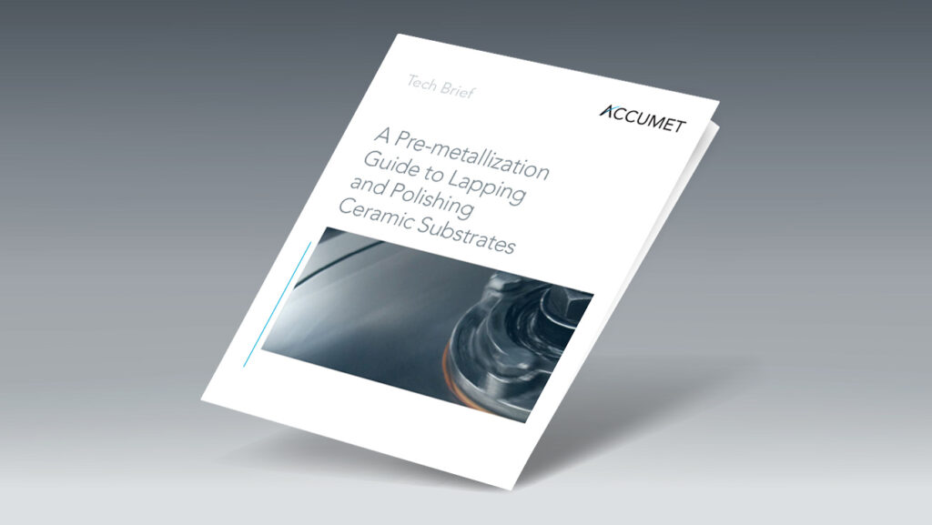
Tech Brief Describes Pre-metallization Benefits of Lapping and Polishing Ceramic Substrates
Posted on December 17, 2018 in Tech Briefs

Lapping, polishing, and grinding are machining techniques that refine a substrate to exact dimensions and tolerances for optimal circuit metallization during both thick and thin film circuit technology procedures. Because the “as-fired”, or as delivered, condition of ceramic, fused silica, or titanate substrates are most often imperfect (wavy, pitted, bumpy, varied in thickness), one or more of these processes is employed to create the exact parallelism, camber, thickness, and surface finish of the substrate material as needed prior to metallizing circuits. This is especially critical to semiconductor manufacturers.
To learn more, download our tech brief:


