Tech Briefs
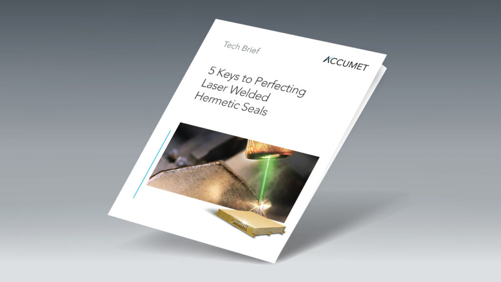
Tech Brief Offers DFM tips for Optimizing Hermetic Seals
Our new tech brief “5 Keys to Perfecting Hermetic Seals with Laser Welding” offers DFM tips for optimizing Hermetic Seals. Hermetic seals are used throughout the high-tech industry to provide maximum packaged protection from environmental elements that can reduce the reliability and required lifetime of critical electronics. Laser welded (or laser fusion welded) hermetic seals…
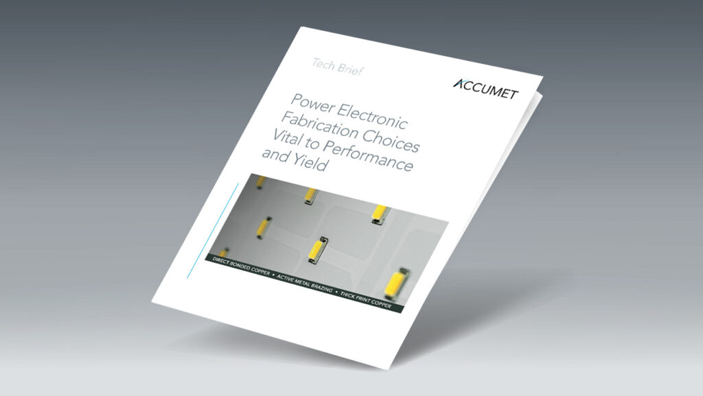
Read MoreTech Brief Describes Fabrication Choices for Power Electronic Performance and Yield
Many solid-state power electronics, including those used in high-powered LED, RF/Microwave, electric vehicle, train and rail, electrical infrastructures, and military applications rely on physically and thermally robust ceramic materials as a base. These ceramic materials are bonded to thermally and electrically conductive metals to help transfer thermal energy to heat spreaders/ heat sinks and away…
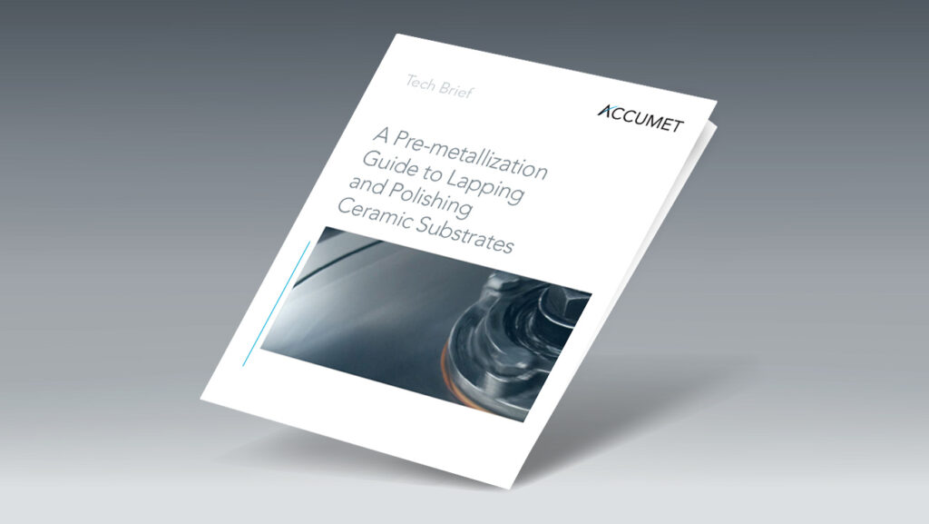
Read MoreTech Brief Describes Pre-metallization Benefits of Lapping and Polishing Ceramic Substrates
Lapping, polishing, and grinding are machining techniques that refine a substrate to exact dimensions and tolerances for optimal circuit metallization during both thick and thin film circuit technology procedures. Because the “as-fired”, or as delivered, condition of ceramic, fused silica, or titanate substrates are most often imperfect (wavy, pitted, bumpy, varied in thickness), one or…
Read MoreTech Brief Provides Keys to Choosing Ceramics and Substrates for High Power Electronics
The latest high power radar systems require both extreme RF power density and longterm reliability, for which careful design and material choices are necessary. This Tech Brief is aimed at high power circuit and system designers, the brief details the common ceramic and semiconductor material choices encountered by designers, and offers insight on the advantages,…
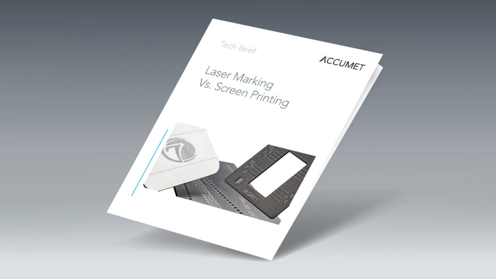
Read MoreTech Brief Describes the Laser Marking Alternative to Screen Printing
Product manufacturers may wish to consider laser marking as an alternative to screen printing (also called silk screening) when looking to permanently mark a surface such as with a bar code, a serial number, a logo, or calibration settings. Depending on the application, laser marking and screen printing each have their pluses and minuses —…
Read MoreTech Brief Describes Laser Ablation as The Alternative to Chemical Etching and Solder Dams
Laser ablation is a process that product manufacturers may wish to consider when looking to remove unwanted materials from a part’s surface or when they wish to control solder flow on a PCB — typically so excess solder does not travel where it’s not supposed to and cause electrical shorting. For cleaning a surface the…
Read More


