IMS Attendees Reported Substrate Processing Becoming Critical in Supply Chain. Stocking Materials and Offering Quick-turn Laser Processing, Viewed as Essential
Posted on June 2, 2017 in Blogs

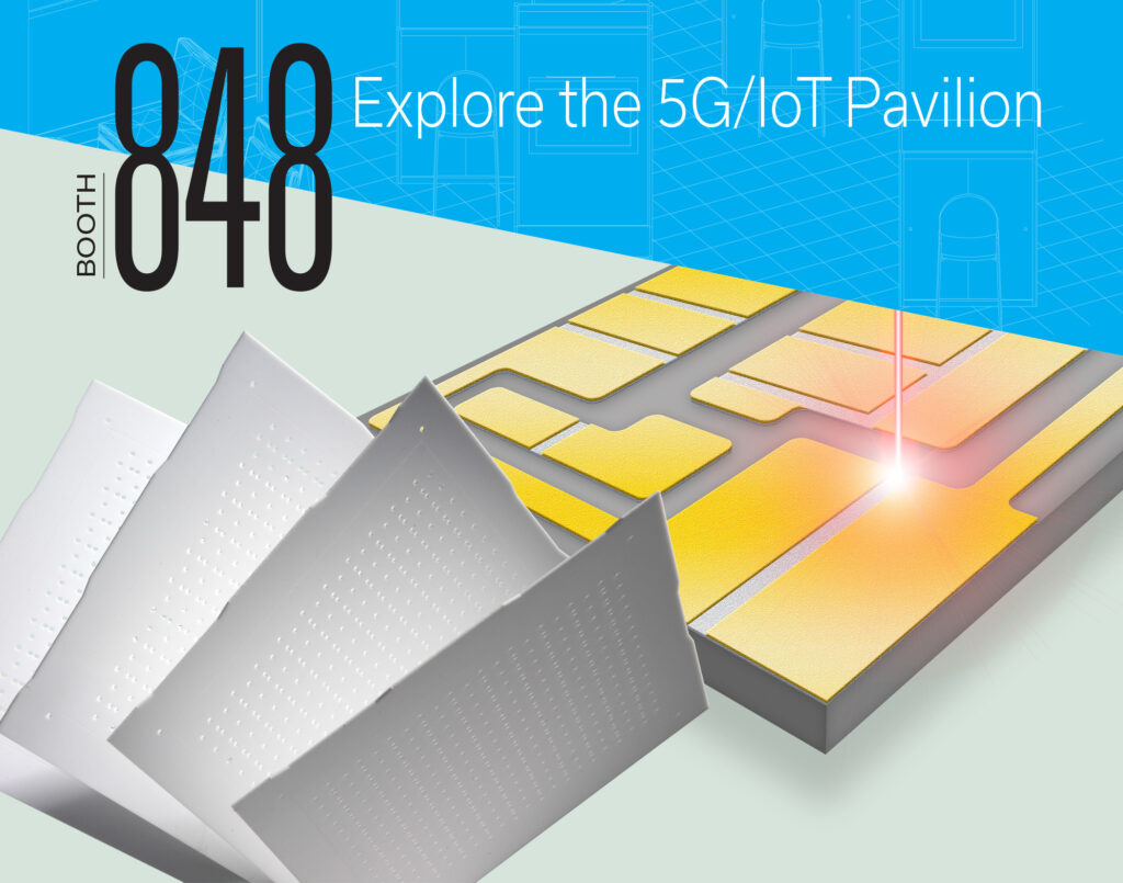
At the 2017 International Microwave Symposium, our two associated brands were discussing the unique substrate and material processing requirements of the RF and microwave industry. What we found was if materials like alumina ceramic from Coorstek, metals, foils, epoxies, microwave absorbers, and other materials are what designers and procurement agents are looking for in a pinch (and they want them to come fully cut, drilled, welded, scribed, etched or marked) a processing partner who stocks these materials becomes an invaluable resource. While material suppliers are often the first source of supply, lead times and minimum orders can throw a monkey wrench into your supply chain when products need to get out the door quickly. Microcircuit manufacturers looking to reduce the cost, time, and materials needed to fabricate their microelectronic circuits are reporting us to be a handy ally. Stocking all major brands of substrate material, Laser Services is an expert at cutting, drilling and scribing; as well as post-processing and ablation. As compared to water-jet cutting which allows for +/- 0.010” feature tolerance, laser cutting can achieve +/- 0.001”.
Our sister company, Accumet, provides ultra-precise lapping, polishing, and diamond cutting of ferrous and non-ferrous metals and ceramic substrates, too. Lapping can be completed from 6 μin to 60 μin and polishing of materials is from 0.1 μin to 5 μin. Accumet can also scribe or dice rectangular or other odd shaped parts up to 0.150” thick in geometries and as small as 0.005” x 0.005”. Accuracy can be held to +/-0.0003”; repeatability to within 0.0001”. Diamond machined edges/ bevels and chamfers can be machined within 0.0005”.
Several technical resources to aid RF and microwave circuit designers in preparing for these process steps can be found at www.laserservicesusa.com/support, including a Tech Brief on how to and where to locate circuit features, and when to include singulation methods, metallization steps, and what material properties and their best applications are.


