Design Guidelines
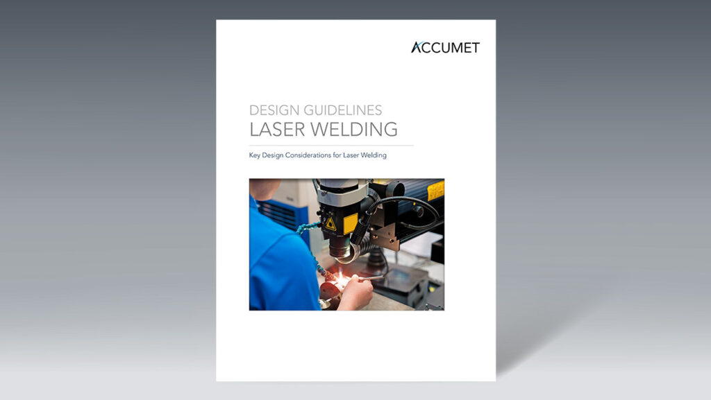
Design Guidelines: Laser Welding
“Laser” stands for Light Amplification by Stimulated Emission of Radiation. Simply put, laser welding uses a laser’s energy to generate heat in a focused beam. The beam is focused on a designated area, and energy is then pulsed through the beam and directed at that area. The beam causes the metal or metals to heat…
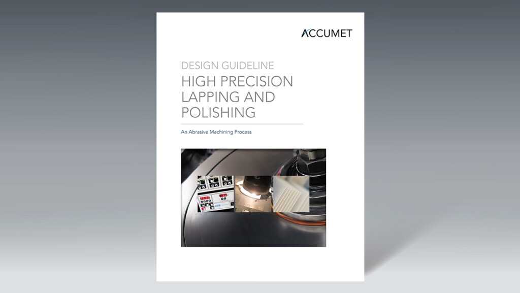
Read MoreHigh Precision Lapping and Polishing Design Guidelines
Lapping and Polishing are processes which are performed to achieve a desired surfaced finish, thickness, parallelism and flatness of any substrate. An application may warrant highly demanding tolerances that off-the-shelf stock or “as-fired” material simply cannot achieve. Accumet has developed several unique substrate lapping machining processes that achieve extremely tight tolerances while offering repeatability from piece to piece.…
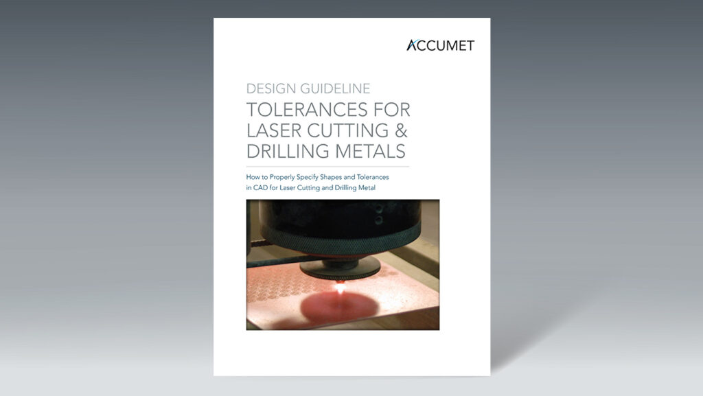
Read MoreDesign Guideline Offers Tolerances for Achieving Ultimate DFM While Processing Metals as Thin as 0.005
Nobody likes being the culprit of rework. That’s why design for manufacturability (DFM) is a key skill for any design engineer. But as devices get smaller and the intricate details get closer together, DFM becomes an art form. For electro-mechanical engineers looking for perfection while working with processed metals, getting tolerances dead-on perfect at the…
Read MoreDownload our Design Guideline: Optimal Tolerances and Layouts for Laser Processing Ceramic Substrates
When RF designers are weighing material choices and considering circuit design during prototype development, Accumet’s material and process engineers are available to help make the right decisions about optimal tolerances and layouts for laser processing ceramic substrates. You can tap into Accumet’s extensive knowledge of ceramic substrates and RF materials, circuit design, anticipated yield loss, attainable…
Read More


